M1 RC1 signal integrity measurements
From Milkymist Wiki
Contents |
[edit] Setup
Measurements were carried out using an Agilent 20Gs/s oscilloscope with a 6 GHz bandwidth and a 7 GHz Agilent differential probe.
Two boards were used:
- Board A is the original RC1, with no modification (original decoupling capacitors and 33 ohm DDR series resistors)
- Board B has the DDR series resistors replaced with 49 ohm resistors and additional 100uF capacitors were installed on C165 and C161 and 100nF capacitors on C162, C166, C159 and C160. The original capacitors were still present and the installed capacitors were soldered in parallel (on top of them).
[edit] Power supply
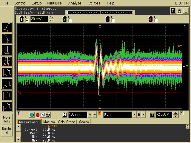
Measurements show that the decoupling capacitors of the DDR are a bit weak. The spike depicted below happens when the DRAM is refreshed; transfers cause similar (but less marked) transients.
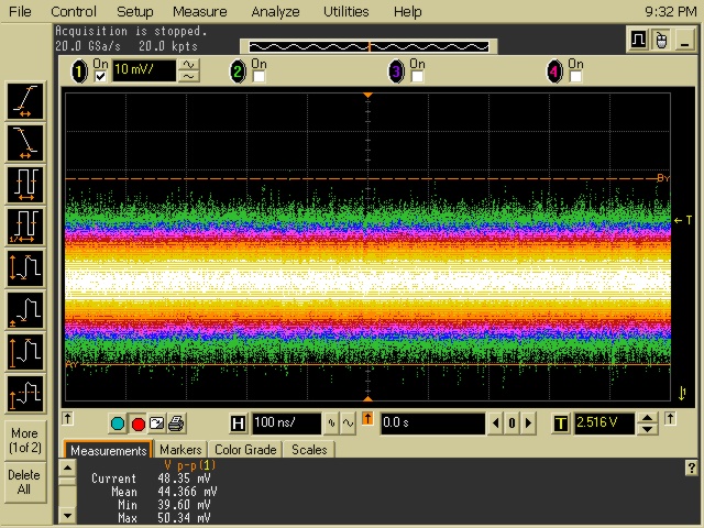
Board B with the additional capacitors has less noise in the power supply.
[edit] Measurements at the C165 pins
[edit] Board A
A transient of roughly 100mV peak to peak is present.
[edit] Board B
The additional 100uF capacitor effectively removes the voltage transient at its pins.
[edit] Measurements at pins 1 and 6 of U14
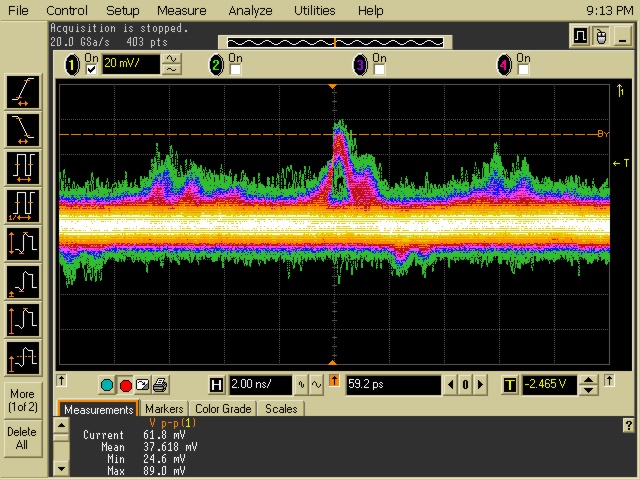
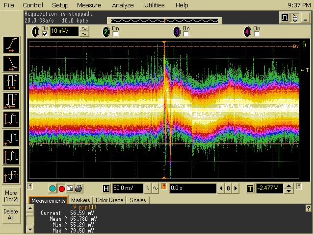
Again, noise and transients are present, but not as marked as on C165. From the measurements taken, the extra capacitors' effect is unclear.
[edit] Board A
[edit] Board B
[edit] DDR clock
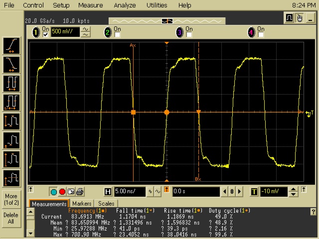
Measured on the board A only, the DDR differential clock is clean and meets the amplitude requirement of the DDRAM datasheet (see p. 21). Individual signal measurement was not performed.
[edit] Address line
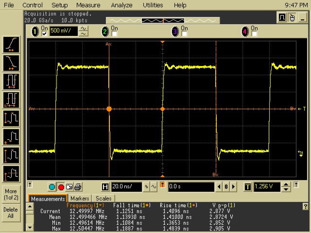
Measurement was taken on the A5 line of U15 with the FPGA transmitting a continuous 12.5MHz square wave using the SSTLII class I I/O standard. Using the 49 ohm resistor results in less overshoot, but also slower rise and fall times.
[edit] Board A
[edit] Board B
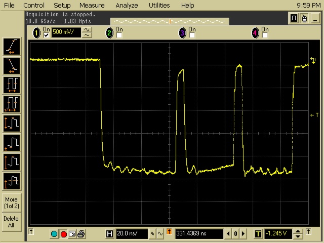
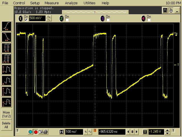
[edit] Data line
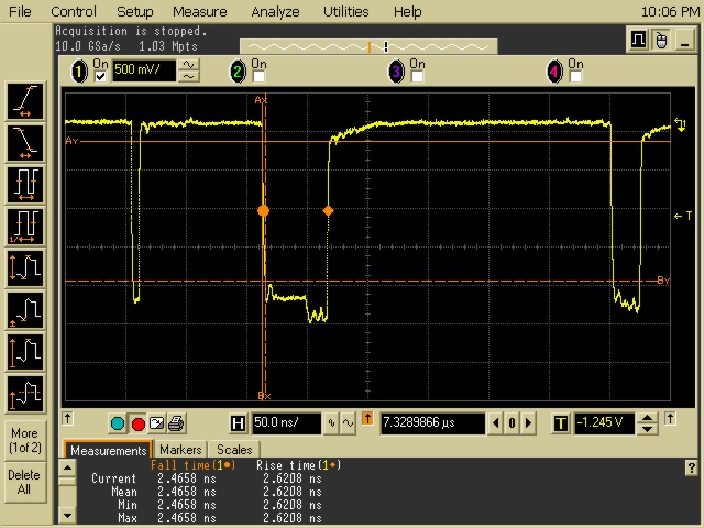
The DQ14 pin at the U15 DRAM was measured on board A with the demo firmware running on SoC v0.8. The DRAM and the FPGA are alternatively driving the pin. The scope probe was inverted so the zero point is actually at the top. Slow transistions of the signal to 0 correspond to the DQ line being tri-stated and discharging. Measurements do not expose particular signal integrity problems on DQ.
